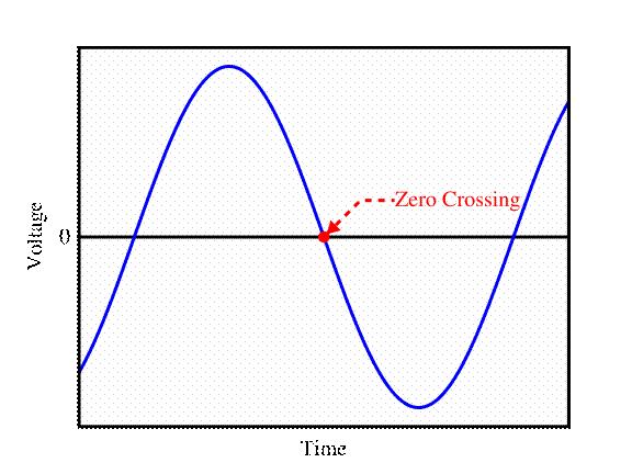
I. Zero-Crossing
By definition, zero crossing is the instantaneous point at which there is no voltage present. This normally occurs twice during each cycle in a sine wave or other simple waveform. The zero crossing is important for systems that send digital data over AC circuits (i.e. home automation control systems and Digital Command Control type systems). Zero crossing is illustrated by the image below:
Figure 8: Zero Crossing Illustration
In a system where an amplifier with digitally-controlled gain is applied to an input signal, signal artifacts will occur when the gain of the amplifier abruptly switches between its discrete gain settings while outputting a non-zero current. This results in artifacts, which are disconcerting and should be eliminated if possible. If changes are made at a zero crossing of the signal, the input is zero, so no matter how the amplifier gain setting changes, the output will also remain at zero. When the power is switched only when the voltage is crossing zero there is no electrical noise generated. This is called zero switching and results in a clean on/off switching pattern.
II. The Thyristor
The thyristor is a solid-state semiconductor device with four layers of alternating N and P-type material. They act as a switch, conducting when their gate receives a current pulse, and continue to conduct for as long as they are forward biased.
Originally proposed by William Shockley in 1950 (referred to as the Silicon Controlled Rectifier or SCR) and championed by Moll and others at Bell Labs and was developed first by power engineers at General Electric (G.E.) led by Gordon Hall and commercialized by G.E.'s Frank W. "Bill" Gutzwiller.
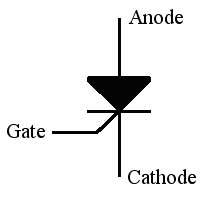
Figure 9: Thyristor SymbolThe thyristor is a four-layer semiconducting device, with each layer consisting of an alternately N-type or P-type material, for example P-N-P-N. The main terminals, labeled anode and cathode, are across the full four layers, and the control terminal, called the gate, is attached to p-type material near to the cathode.
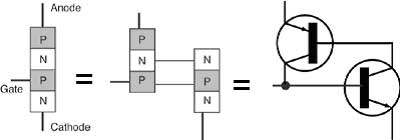
ANALOGY:
Thyristor operation = 2 BJT tightly coupled and arranged to cause the self-latching action.
Figure 10. Thyristor Operation
Thyristors have three states:
- Reverse blocking mode -- Voltage is applied in the direction that would be blocked by a diode
- Forward blocking mode -- Voltage is applied in the direction that would cause a diode to conduct, but the thyristor has not yet been triggered into conduction
- Forward conducting mode -- The thyristor has been triggered into conduction and will remain conducting until the forward current drops below a threshold value known as the "holding current"
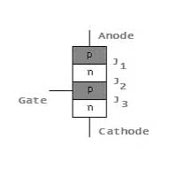
Function of the gate terminal
The thyristor has three p-n junctions (serially named J1, J2, J3 from the anode).
If VAK is positive with respect to the cathode and VG = 0, then J1 and J3 are forward-biased, while junction J2 is reverse-biased. As J2 is reverse biased, no conduction takes place. If VAK is increased beyond the breakdown voltage VBO of the thyristor, avalanche breakdown of J2 takes place and the thyristor starts conducting.
If VG is positive with respect to the cathode, then breakdown of the junction J2 occurs at a lower value of VAK. By selecting an appropriate value of VG, the thyristor can be switched into the on state immediately.
It must be noted that VG need not be applied after the avalanche breakdown has occurred. Hence VG can be a voltage pulse, such as the voltage output from an UJT relaxation oscillator.
These gate pulses are characterized in terms of gate trigger voltage (VGT) and gate trigger current (IGT). Gate trigger current varies inversely with gate pulse width in such a way that it is evident that there is a minimum gate charge required to trigger the thyristor.
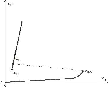
Switching characteristics
Figure 11. Switching CharacteristicIn a conventional thyristor, once it has been switched on by the gate terminal, the device remains latched in the on-state, providing the anode current has exceeded the latching current (IL). As long as the anode remains positively biased, it cannot be switched off until the anode current falls below the holding current (IH).
A thyristor can be switched off if the external circuit causes the anode to become negatively biased. In some applications this is done by switching a second thyristor to discharge a capacitor into the cathode of the first thyristor. This method is called forced commutation.
After a thyristor has been switched off by forced commutation, a finite time delay must have elapsed before the anode can be positively biased in the off-state. This minimum delay is called the circuit commutated turn-off time (tQ). Attempting to positively bias the anode within this time causes the thyristor to be self-triggered by the remaining charge carriers that have not yet recombined.
For applications with frequencies higher than the domestic AC mains supply (e.g. 50Hz or 60Hz), thyristors with lower values of tQ are required. Such fast thyristors are made by diffusing into the silicon heavy metal ions such as gold or platinum which act as charge combination centers. Alternatively, fast thyristors may be made by neutron irradiation of the silicon.
Types of Thyristors
- Silicon controlled rectifier (SCR)
- ASCR — asymmetrical SCR
- RCT — reverse conducting thyristor
- LASCR — light activated SCR, or LTT — light triggered thyristor
- DIAC & SIDAC — both forms of trigger devices
- BOD — breakover diode — a gateless thyristor triggered by avalanche current, used in protection applications
- TRIAC — a bidirectional switching device containing two thyristor structures
- GTO (thyristor) — gate turn-off thyristor
- MA-GTO — Modified anode gate turn-off thyristor
- DB-GTO — Distributed buffer gate turn-off thyristor
- MCT — MOSFET controlled thyristor containing two additional FET structures for on/off control.
- BRT — Base Resistance Controlled Thyristor
- SITh — Static induction thyristor, or FCTh — Field controlled thyristor containing a gate structure that can shut down anode current flow.
III. Firing of the Thyristor

Figure 12: Complete Firing Circuit
The first part of the circuit involves the rising of the ramp from the zero-crossing as well as timing the firing of the thyristor. The upper part of the circuit produces the ramp. The point of the ramp generator is to generate a linear ramp that starts out at 0 volts and increases (linearly, of course) until the zero-crossing of the input, when it gets reset and starts over again. This gives a sawtooth wave synchronized with the zero-crossings.
Given that R2 has a value of 4KΩ and the voltage across it is 4V, the current across R2 is 1 mA. This current goes through capacitor C1 and makes a ramp. The rate of the rise of the ramp is dictated by the following equation:
θ=Cv= it
where C is the value of capacitor C1, v is the 2/3 of the voltage of the Vcc of the 555, i is the current passing through the capacitor and t is the time that the thyristor will be fired. We get 2/3 of the 555’s Vcc because pin 6 will fire if the voltage gets past that point. Diode D1 prevents the 555 from breaking down when the voltage at the emitter is 5.6 V.
The frequency of the input is 60 Hz, therefore the period is 1/60=16.7 ms. The thyristor will be able to fire at any time within the first 8.35 ms. The given value of C1, 5μF, gives a t=16.7 ms. Assuming that the earliest time to fire the thyristor can be taken at 10% of 8.35ms or 0.8ms, C1 should instead be given the value 0.25μF. The earlier we fire, the greater the energy sent to the bulb and the brighter the bulb will be.
Pin 7 of the 555 is an open collector output. When the voltage at the capacitor increases, pin 6 fires, and pin 7 conducts, discharging the capacitor. Diode D2 ensures that the capacitor will not charge at the wrong time. When pin 3 or A is 0, E becomes 1, and X is also 1. If Y is 1, then Z is 0. Placing a 0 at Y resets the latch and allows the charging of the capacitor.
Going to Q2, R4 ensures that the gate won’t be wrecked by dropping the voltage by 0.5 V.
The part of the circuit with the transformer involves rectifying the AC for a pulsating DC. We need the inverse signal as an input for Y. If the signal falls to 0, the latch will reset and the capacitor will charge. This part of the circuit involves a full-wave rectifier (as implemented with the four diodes), followed by an inverter (implemented by transistors Q3 and Q4.
The circuit uses AC power. The AC power is applied at the zero-crossing point to minimize noise spikes due to abrupt changes in the drive signal. Only a minimal amount of power is used to maintain the set value.