|
1
|
go to top
next
previous
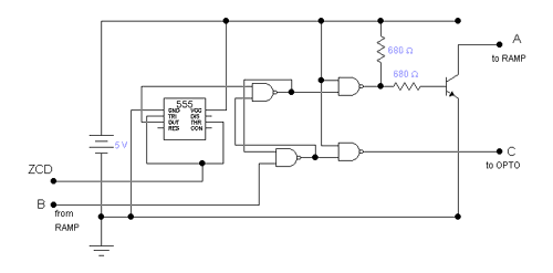
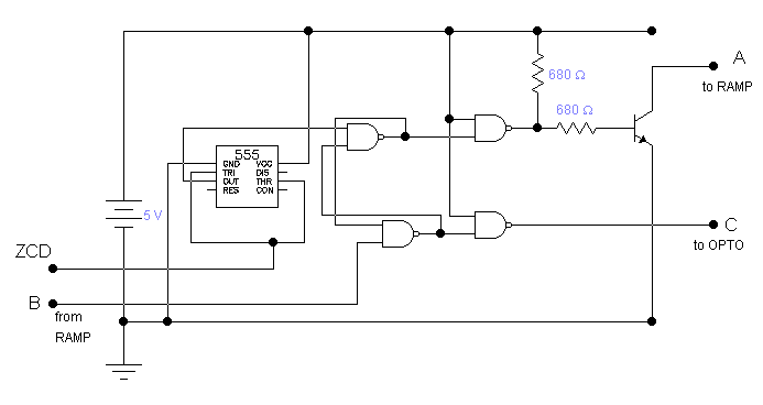
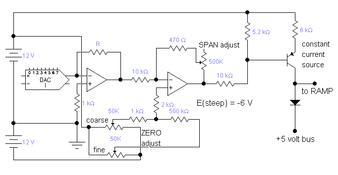
"Input ZCD".
The circuit takes its input from the "zero-crossing detector", which provides it with a 0-to-1-to-0 pulse to "set" the R-S flip-flop and release the ramp circuit (A to Ramp) for it to start the ascent of the timing ramp.
"Input B from Ramp".
After the ramp has risen to the predetermined timing voltage, it sends a 1-to-0-to-1 pulse back to this circuit to "reset" the R-S flip-flop.
"Output A to Ramp".
"Input ZCD" signals the start of the timing ramp.
"Output C to Opto".
At the time that "Input B" comes, this circuit sends a trigger firing signal to the gate of the thyristor to signal conduction.
|
|
|
|
2
|
go to top
next
previous
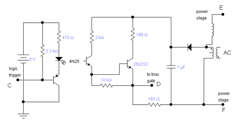
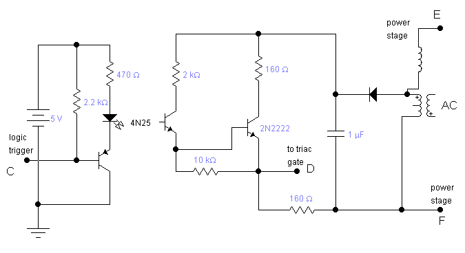
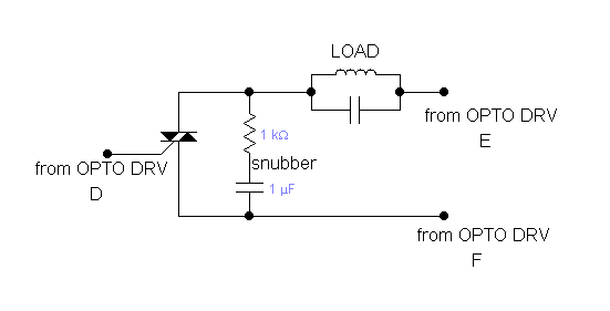
"Input C" and "Output D".
"A low signal at "Logic Trigger C" will produce "source" current at "D".
"Power Supply".
The diode produces power to supply the requirements of the circuit to provide the source current to the gate of the thyristor.
Terminals "E" and "F".
These alternating current terminals provide the supply power to the thyristor and its test load.
|
|
|
|
3
|
go to top
next
previous
.
.
.
|
|
|
|
4
|
go to top
next
previous
.
.
.
|
|
|
|
5
|
go to top
next
previous
.
.
.
|
|
|