thyristor trigger interlock Sample Circuits
trigger interlock


1 go to top      next      previous

A negative-going edge comes into the input node, and is differentiated by the input circuit to pin #2 of the 555. The input brings pin #2 below 1/3 of Vcc, to which the 555 reacts to bring its output pin #3 to logic "1" and its open-collector pin #7 out of conduction. This action at pin #7 will case the resistor to charge the timing capacitor connected to pin #6.

The capacitor charges beyond 2/3 of Vcc, causing pin #6 to sense the fact and force pin #3 to logic "0" and the open-collector transistor at pin #7 to conduct, discharging the capacitor and bringing the capacitor voltage near the negative rail.

The process will be repeated with the coming of the next input of a negative-going edge.

Note that there will be need to provide a reverse-biased diode at pin #2 to Vcc to prevent this input structure from undergoing unnecessary stress from the positive pulse component of the differentiated signal, i.e., when the input signal becomes a positive-going edge.
 
  back to whole circuit
2 go to top      next      previous

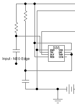
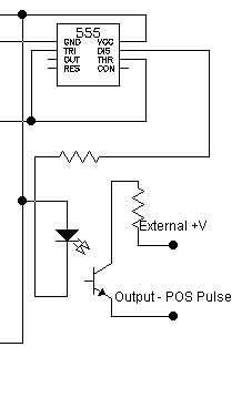
The logic "1" output of the preceeding stage above will bring pin #2 and pin #6 high, causing pin #7 of this 555 to conduct and bring the cathode of the LED down causing current to stimulate the emission of light to the base of a light-sensitive transistor, causing it to conduct, as well.

With this process, current from the emitter will be sent to the gate of a thyristor, causing it to conduct for the rest of the alternating-current cycle. The process will be repeated with the introduction of another negative-going edge at the input.

Note that, once triggered, the thyristor will maintain conduction until the current falls below the physical "latching current of the thyristor.
 
  back to whole circuit
go to top