|
1
|
go to top
next
previous
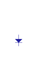
The diode is a device that allows current from the anode ("A") to the cathode ("K").
Rule of Thumb: A silicon diode will present a 0.6-volt drop between the anode and the cathode. In other words, the anode will be more positive than the cathode by about 0.6 volts.
If the rating of a diode is not known, the current that will bring this voltage drop to about 0.85 V could be taken as the maximum continuous forward-biased rating of this diode.
A normal laboratory inventory would, typically, carry two types of diodes, namely, the signal and the power diodes. The signal diode is usually encased in glass. Compared to a power diode, it is able to switch (change from conduction to non-conduction, and vice-versa) in a relatively shorter span of time, and has a lower current-carrying capacity. My designs limit sustained currents to no more than 20 ma on signal diodes.
Power diodes, on the other hand have higher current ratings, and are usually slower.
All diodes "break down" (conduct), when reverse-biased beyond some voltage. This voltage is higher than the diode's rated PIV (peak inverse voltage).
|
|
|
|
2
|
go to top
next
previous
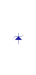
If forward-biased, a zener diode behaves in almost exactly the same way as the ordinary diode.
The characteristic that distinguishes it from a regular diode is that it conducts at a lower "reverse bias" voltage. A zener diode is rated at this reverse bias voltage.
The power dissipation is an important rating. It is the product of the "zener breakdown voltage" and the "current passing through the zener diode at this voltage". Thus a zener diode rated at 6 volts and 0.5 watt will be able to carry 4 times the current of a similar zener diode rated at 24 volts and 0.5 watt.
The relevant equation is Power = Voltage * Current.
|
|
|
|
3
|
go to top
next
previous
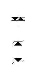
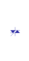
A diac behaves similar to a zener diode. A diac has two terminals, say MT1 and MT2. It will conduct at a zener voltage, Vz, when MT1 is at a more positive potential than MT2. In this regard, its behavior is similar to that of a zener diode. However, it will also conduct at the same Vz when MT2 is more positive than MT1.
Its behavior could almost be described as similar to two "back-to-back" zener diodes in the diagram at the right.
The calculation of a diac's power dissipation is the same as that of a zener diode's.
|
|
|
|
4
|
go to top
next
previous
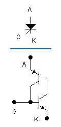
The lower diagram is a simplified way of explaining the behavior of an SCR if one is already acquainted with the NPN and the PNP transistors. A current ("gate current") applied to the base-emitter junction will cause the NPN transistor to conduct. This conduction will cause a collector current at the NPN transistor to introduce a base-emitter current at the PNP transistor. Such a state will cause the PNP transistor to conduct and feed bias current back to the NPN transistor.
This positive re-enforcement ("feedback") is likened to a very fast chain reaction, which quickly changes the impedance of A-K from a very high value before the trigger signal to a very small value after the trigger is applied.
The external behavior of the SCR is almost exactly like that of the transistor pair. The internal physics, however, is something else.
Thyristors, among this class is the SCR, have ratings that are important to the practical designer. Aside from the usual voltage and current ratings, the two more important ones are:
- "Critical dv/dt" - This is related to the increase in the potential difference between the Anode and the Cathode when the SCR cuts off. When the actual circuit dv/dt is too large, the internal circuit values would tend to cause the SCR to conduct, thus making the circuit malfunction. In the absence of a specific ratings sheet, the circuit could be designed so that the dv/dt value is limited to about 10 to 20 volts per microsecond.
- "Critical di/dt" - This is related to the amount of current at initial conduction. A di/dt which is higher than the rating of the device could cause overheating of the "semi-conductor junction", causing the device to fail. Unlike the dv/dt value above, one will need to consult the manufacturers specifications. In the most extreme case that one has to apply a solution, and if the circuit can take it, one could be safe with full current reached 75 microseconds from the time the gate is triggered. Actual applications and trouble-shooting demands do not usually require that one will need to go into this exercise.
|
|
|
|
5
|
go to top
next
previous
The
|
|
|