Hardware Implementation
Zharlou T. Panganiban
back to CE150
The Hardware part of this project consists of the parallel port interfacing and the transmitter interfacing. The first part is concerned with setting up the needed hardware precautionary measures for safe and proper parallel port interfacing. The schematic diagram below shows the circuit used for safeguarding the parallel port from feedback signals coming from the interfaced device.
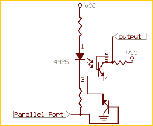
Figure 1. Interface circuit for one pin in the parallel port.
Optoisolators are used to guard the port by isolating it from the external device. In the schematic diagram, it is shown that optoisolators are mainly composed of an LED and a photodiode. If there is an input in the Vcc node and no output in the parallel port, the LED is biased, and it gives off light. This light induces a current in the phototransistor. It will then create a voltage drop, and the voltage read at the output is at ground level. If there is an output voltage in the parallel port, then the LED is not biased. No current will be induced in the phototransistor and thus, the voltage read at the output is the Vcc node.
This circuit is duplicated four times since there are four pins used for this project. This corresponds to the four basic commands used: GO, BACK, LEFT and RIGHT. No more pin is assigned to the STOP command, since the four pins are used for this specific command; the four pins are reset once this command is executed. The orcad-pcb design for the whole interface is shown below.
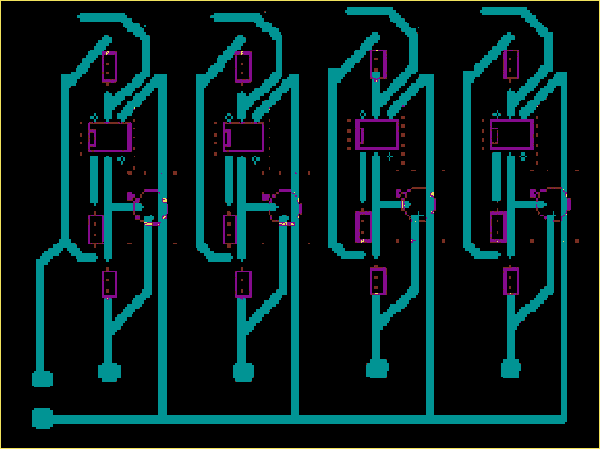
Figure 2. ORCAD-PCB design for the parallel port interface
|