Analog Switching Circuit TOP
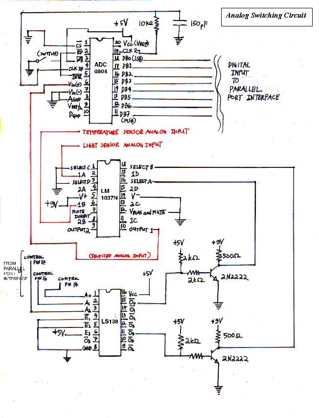
This circuit converts the 0-5 V analog signal from the light and temperature sensors into digital form (8-bits) ready for input into the computer. Using only one analog-to digital converter (ADC0804), the proper analog signal from the specific sensor selected is made available through the analog switch (LM1037N) output. The demultiplexer (LS138) and 2N2222 transistor circuits are used to convert the input control line combination (Pins 14, 16, and 17 from the PC) to make the proper sensor selection. They are necessary since the LM1037N is not a standard TTL device. To make a selected analog input appear at the proper output pin, the select pin for that input must be brought to the same voltage as that of its supply (V+ pin). However, the switching does not occur properly (output is clipped at 4 Volts) for a supply voltage of +5 Volts which is the standard for TTL devices. Thus, a supply of +9 Volts is used. The transistor circuits are there to set the TTL output from the demultiplexer to the proper +9 Volt level needed to make a successful input selection for the analog switch. The selected output at the demultiplexer will be at logic low, while the rest of the outputs are high. This brings the output from the 2N2222 circuit to a high of +9 Volts, and this is fed into the proper analog switch select pin.
The analog-to-digital converter is set to run in free running mode. The resistor-capacitor circuit is there to provide its own internal clock. There is also a switch connecting the INTR and READ pins to ground. The free-running mode of the ADC requires this, tying the two pins together, and setting them momentarily to ground to enable the ADC to function. In our experimentation, we have found that the switch acted like a reset switch for the ADC when a surge of current (or some other thing) due to a reading higher than 5 Volts from the analog input would cause it to suddenly malfunction.
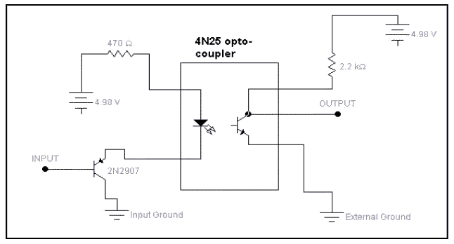
Optocoupler Circuit TOP
Parallel Port Interface TOP
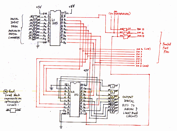
Although used the standard use of the 8 parallel port data lines (Pins 2 to 9) is just for output, the proper BIOS setting and software commands could allow its use for input as well. Thus, there was a need to make the connections to these 8-data lines "two-state", to allow for both input and output. Since it would be difficult to come up with a two-way optocoupler array, it was decided that the "two-way" implementation come between the parallel port pins and the optocouplers used to protect the PC from external stray current. The implementation consists of a buffer (LS245) to allow for input, and a latch (LS373) for the output. The output pins/lines of the buffer are tied to the corresponding input lines of the latch, and these common lines are connected to the corresponding parallel port data pins. The latch enable pin and the buffer high impedance at output pin are controlled separately by a specific control line from the PC (either pin 16 or pin 17) so as to allow proper switching between input and output.
TOP
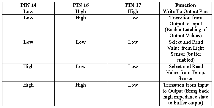
The control line combinations and their corresponding functions are the following:
The light bulb and air-con control make use of the output data bits. Their connections come after the output optocoupler array. The two least significant output bits are used to control the air-conditioning unit, one bit setting the main fan, and the other, the compressor. The other six data bits are used to control the light bulb, from turning it on to controlling its light intensity.
Each element of the optocoupler arrays in the interface circuit (represented as a box with "in" and "out" labels) is constructed as drawn out in the circuit diagram preceding the interface circuit. Perhaps we may have implemented "protection" of the PC from external surges in the wrong way as all our grounds were tied to the PC ground. However, at least for the data lines and control lines, assuming the buffer and latch are "safe", there is considerable isolation from the external circuits.
|